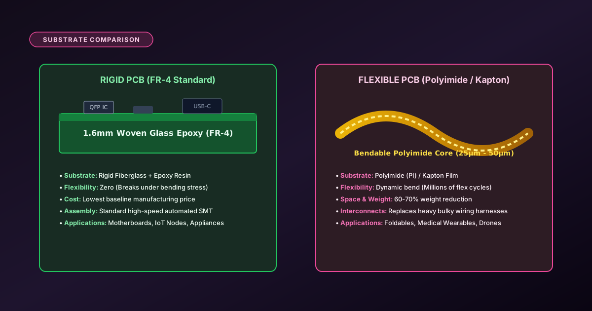
What is a Flexible PCB (FPC)?
- [Polyimide Kapton Film] [replaces] [rigid fiberglass epoxy to enable mechanical flexing and high heat resistance]
- [Flex Circuit Interconnects] [eliminate] [bulky discrete wire harnesses, crimp terminals, and assembly labor]
- [IPC-2223 Design Standard] [mandates] [minimum bend radii, curved trace routing, and cross-hatched ground copper]
While traditional rigid PCBs rely on thick (0.8mm – 1.6mm) woven fiberglass cloth bound with brittle epoxy resin (FR-4), flexible printed circuits utilize high-performance Polyimide (PI) films measuring only 12.5 µm to 50 µm (0.5 to 2.0 mils) in thickness.
Polyimide (commercially known as DuPont Kapton) offers an exceptional combination of tensile strength, thermal endurance (operating from -200°C to +300°C without melting), and extreme fatigue resistance. A properly engineered 1-layer flex circuit can withstand more than 10,000,000 continuous flex cycles in a laptop display hinge or camera gimbal without a single copper trace fracture.
Flex PCB Design for Manufacturing (DFM) Rules
Designing flexible circuits requires a fundamental shift in layout methodology. Standard rigid PCB layout habits (like 45-degree angled traces and solid copper pours) cause catastrophic mechanical failure on flexible substrates:
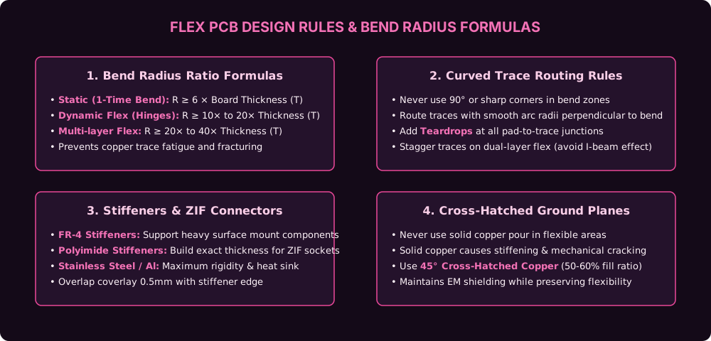
1. The Bend Radius Formulas (IPC-2223)
The minimum permissible bend radius (R) depends on the total board thickness (T) and the operational nature of the bend:
- Static (Flex-to-Install / 1-Time Bend): R ≥ 6 × T (Single-layer) | R ≥ 12 × T (Multi-layer)
- Dynamic (Continuous Cycling / Hinges): R ≥ 10× to 20 × T (Single-layer only)
- Multi-Layer Dynamic: R ≥ 20× to 40 × T (Avoid dynamic flexing on > 2 layers)
2. Curved Traces & Teardropping (No Sharp Corners)
Never route traces with sharp corners or 45-degree chamfers in flexible zones. Always use smooth, circular arc curves oriented perpendicular to the bend axis. Apply teardrop fillets at every pad-to-trace junction to distribute mechanical shear strain during bending.
3. Staggered Traces on 2-Layer Flex (Preventing the I-Beam Effect)
If copper traces on the Top and Bottom layers are routed directly on top of each other, they form an "I-Beam" cross-section that drastically stiffens the board and concentrates stress on the outer copper layer. Always offset/stagger top and bottom traces so they do not overlap vertically in bend regions.
4. 45° Cross-Hatched Copper Pours
Solid ground copper pours will wrinkle, delaminate, and crack when bent. Use a cross-hatched ground plane pattern oriented at 45 degrees with a 50% to 60% copper fill factor. This maintains electromagnetic shielding and continuous return paths while preserving maximum flexibility.
Rigid PCB vs Flexible PCB vs Rigid-Flex: Shootout Table
| Feature / Attribute | Rigid PCB (FR-4) | Flex PCB (Polyimide) | Rigid-Flex Hybrid |
|---|---|---|---|
| Substrate Core | Woven Glass + Epoxy (FR-4) | Polyimide (Kapton) Film | Integrated FR-4 + Polyimide |
| Flexibility & Bend Life | Zero (Brittle, will snap) | > 10 Million Dynamic Cycles | Dynamic in Flex Zones |
| Thickness Range | 0.8 mm – 3.2 mm (Std 1.6mm) | 0.05 mm – 0.2 mm (Ultra-thin) | 1.6mm Rigid / 0.15mm Flex |
| Weight & Space Savings | Baseline standard | 60% to 70% lighter & thinner | 50% reduction in cabinet size |
| Interconnect Reliability | Requires wire harnesses/headers | Direct ZIF / Board-to-board | Monolithic (Zero connectors) |
| Unit Fabrication Cost | $ (Lowest baseline cost) | $$ (2x – 3x higher than rigid) | $$$$ (Highest tooling cost) |
| Assembly Complexity | Standard automated SMT | Requires carrier trays / pallets | Multi-stage SMT process |
| Primary Applications | Motherboards, IoT nodes, PSU | Cameras, Wearables, Foldables | Aerospace, Military, Medical |
Stiffeners & Coverlays: Structural Reinforcement
Because flexible polyimide film is only 25µm to 50µm thick, it cannot directly support heavy components or withstand repeated insertions into edge connectors without reinforcement:
FR-4 Stiffeners (0.5mm – 1.6mm)
Applied underneath surface-mount ICs, microcontrollers, and SMD passives. Prevents the flex film from bowing during reflow soldering and protects delicate solder joints from fatigue stress.
Polyimide Stiffeners (0.1mm – 0.3mm)
Laminated on the back side of ZIF (Zero Insertion Force) connector contact fingers to build up the exact standard thickness (e.g., 0.30 mm ± 0.03 mm) required for secure mechanical latching.
Stainless Steel / Aluminum Stiffeners
Used when extreme mechanical rigidity, electromagnetic shielding, or localized heat sinking is required in high-power sensor applications.
Flex PCB & ZIF Connector Sourcing in India
Hardware developers building wearables, foldable devices, and camera gimbals in India can source FPC prototypes, ZIF connectors (0.5mm / 1.0mm pitch), and custom flex cables from domestic and local markets:
Bangalore
ZIF FPC connectors (0.5mm / 1.0mm pitch), Polyimide Kapton tape rolls, rapid 1-layer flex prototype orders
Mumbai
Wearable medical electronics components, high-density FPC breakout boards, laser stencil services
Delhi NCR
Consumer electronics camera module ribbons, drone gimbal flexible flat cables (FFC), ultrasonic welders
Chennai
Automotive sensor flex harnesses, high-temperature polyimide film suppliers, precision crimping tools
Hyderabad
OLED display FPC connectors, smart watch biometric sensor breakouts, flexible battery interconnects
Pune
Industrial robot joint flexible cabling, automotive dashboard flex circuits, endurance flex cycle testers
Kolkata
FFC jumper cables, display ribbon replacements, student robotics flex sensor materials
Frequently Asked Questions
What is a Flex PCB and how is it fundamentally different from a Rigid PCB?
A Flexible Printed Circuit (FPC) uses a ductile, ultra-thin polymer film (typically Polyimide or Kapton) as its dielectric base instead of rigid fiberglass-epoxy (FR-4). This allows the circuit board to bend, fold, and twist dynamically inside compact 3D enclosures or hinge mechanisms without fracturing the copper traces.
What is the formula for calculating PCB bend radius?
For a static (one-time installation) bend, the minimum bend radius must be R ≥ 6 × T, where T is the total board thickness. For dynamic flexing applications (such as laptop hinges or printer head ribbons that flex repeatedly), the minimum radius must be R ≥ 10× to 20× T for 1-layer flex, and R ≥ 20× to 40× T for multi-layer flex to prevent copper metal fatigue.
Why are solid copper ground pours prohibited in flexible bend zones?
Solid copper sheets drastically increase the mechanical stiffness of the board and create high mechanical shear stress during bending, which causes the copper to buckle, wrinkle, and crack. In flexible zones, engineers always use 45-degree cross-hatched copper pours (50% to 60% fill) to provide electromagnetic shielding while preserving mechanical flexibility.
What are PCB stiffeners and when are they required on flex circuits?
Stiffeners are rigid plates (made of FR-4, Polyimide, or Stainless Steel / Aluminum) laminated onto specific localized sections of a flex board where surface-mount components (SMT), heavy connectors, or Zero Insertion Force (ZIF) contact fingers are located. Stiffeners prevent the flex circuit from bending under mechanical solder joints, preventing solder pad delamination.
What is a Rigid-Flex PCB?
A Rigid-Flex PCB is a hybrid monolithic circuit that integrates rigid FR-4 sections (for mounting dense microcontrollers, BGA processors, and power components) directly unified with flexible polyimide layers (which act as built-in ribbon cables). It completely eliminates external wire harnesses, bulky crimp connectors, and manual soldering.
What is Coverlay on a Flex PCB and how does it differ from Solder Mask?
Standard rigid PCBs use Liquid Photoimageable (LPI) solder mask, which is brittle and will crack under flexing. Flex PCBs use a "Coverlay"—a flexible laminated layer of polyimide film coated with an acrylic or epoxy adhesive that is thermally pressed over the traces, providing permanent moisture, chemical, and mechanical flex protection.
Why should sharp 90-degree trace corners never be used in flex PCB routing?
Sharp corners create severe mechanical stress concentration points during bending, leading to microscopic copper microfractures and premature trace open-circuits. Traces in bend regions must always be routed perpendicular to the bend line with smooth, sweeping curved arcs and generous teardrop pad transitions.
Conclusion: Choosing Between Flex and Rigid Substrates
The choice between Rigid FR-4 PCBs and Flexible Polyimide Circuits depends on packaging constraints, dynamic motion requirements, and budget. While rigid boards remain the most cost-effective solution for standard stationary electronics, flexible and rigid-flex circuits enable the ultra-compact, lightweight, and durable form factors of modern wearables, smartphones, and aerospace hardware.
📚 References & Flexible Circuit Standards
Related Hardware & PCB Guides
How PCB Works
Anatomy, layers, materials and industrial manufacturing process.
How to Design a PCB
Step-by-step EDA guide from schematic capture to Gerber export.
PCB Trace Width Guide
IPC-2152 formulas for current capacity and thermal rise calculations.
4-Layer PCB Stackup
Layer ordering, ground return paths, and low-impedance power routing.