What is a PCB (Printed Circuit Board)?
- [Printed Circuit Board] [replaces] [fragile point-to-point discrete wiring harnesses]
- [Copper Traces] [conduct] [power and high-frequency electrical signals between integrated circuits]
- [FR-4 Dielectric Core] [provides] [high mechanical rigidity and electrical galvanic isolation]
Prior to the invention of printed circuit boards in the mid-20th century by Paul Eisler, electronics relied on point-to-point chassis wiring. Bulky vacuum tube sockets, discrete carbon resistors, and inductors were soldered to terminal strips and bus wires by hand. This produced massive parasitic inductance, unpredictable stray capacitance, loose solder joints, and labor-intensive assembly lines.
Modern printed circuit boards compress complex computing architectures—such as 64-bit microprocessors, multi-gigahertz DDR5 memory buses, and high-density power stages—into monolithic, multilayer structures measured in fractions of a millimeter. By controlling the exact physical geometry of copper conductors and the dielectric properties of isolating substrates, engineers turn physical board traces into precision transmission lines with guaranteed characteristic impedance (50Ω single-ended and 100Ω differential).
The 4 Fundamental Layers of PCB Architecture
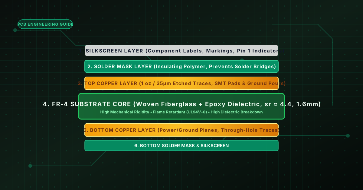
Every standard printed circuit board, whether a simple single-sided board in an AC adapter or a 16-layer motherboard in a high-performance server, is constructed from a sandwich of four primary materials:
1. Substrate Core (FR-4 / Base Dielectric)
The substrate provides structural rigidity and galvanic electrical isolation between opposing copper conductors. The universal industry benchmark is FR-4(Flame Retardant 4), a composite of woven fiberglass cloth impregnated with a brominated epoxy resin binder. FR-4 exhibits a dielectric constant (Dk or εr) between 4.2 and 4.5 and a loss tangent (Df) around 0.02. For high-temperature automotive applications, high-Tg FR-4 (Tg > 170°C) is selected. In RF and microwave circuits operating above 5 GHz, specialized PTFE or ceramic hydrocarbon laminates (such as Rogers RO4350B or Taconic) replace FR-4 to prevent dielectric signal attenuation.
2. Conductive Copper Foil Layer
An electrodeposited or rolled-annealed layer of pure electrolytic copper is thermally bonded to the substrate under heat and vacuum pressure. Copper weight is specified in ounces per square foot (oz/ft²). A 1 oz copper layer measures 35 µm (1.37 mils) in thickness, while 0.5 oz measures 17.5 µm and 2 oz measures 70 µm. Copper tracks are chemically etched to form point-to-point connections, surface mount pads, thermal dissipation slugs, and expansive ground shield pours.
3. Solder Mask Layer (Solder Resist)
A liquid photoimageable (LPI) epoxy polymer is applied over the etched copper traces. The solder mask serves two critical purposes: it provides permanent environmental isolation against oxidation, moisture, and dust; and it prevents solder from forming unintended electrical bridges between tightly spaced adjacent component pins during wave soldering or automated reflow ovens. Solder mask is photographically cleared away only over component solder pads, test points, and mounting holes.
4. Silkscreen Legend Layer
The topmost layer consists of high-contrast, non-conductive epoxy ink printed via automated direct legend printing (DLP) or screen stencils. Silkscreen markings display component reference designators (e.g., C1, R10, U4), pin-1 polarity indicators for ICs and electrolytic capacitors, company branding, board revision tags, and terminal block voltage ratings for maintenance engineers and assembly line operators.
How Current Flows Between Layers: Vias Explained
In multi-layer printed circuit boards, signals and power rails must transition vertically across different copper planes. This is accomplished using Vias (Vertical Interconnect Access)—microscopic drilled holes whose inner cylindrical walls are electroplated with a 20–25 µm barrel of pure copper.
Key Types of PCB Vias:
- Standard Through-Hole Via: Drilled completely through the board from top to bottom using mechanical CNC carbide drill bits. It is the most robust and economical via type, though it consumes routing real estate on every internal layer it passes through.
- Blind Via: Connects an external surface layer to one or more internal layers without penetrating through the opposite side. Created using controlled-depth mechanical drilling or UV lasers during lamination stages.
- Buried Via: Resides entirely inside the internal layer core, connecting internal routing layers with zero exposure on the top or bottom surfaces.
- Microvia (HDI):Laser-drilled holes with diameters < 150 µm spanning a single dielectric layer, commonly used in high-density interconnect (HDI) smartphones and 0.4mm pitch BGA processors.
- Thermal Vias: Clusters of conductive vias placed directly underneath power MOSFETs and voltage regulators to conduct heat away into large internal ground copper planes.
The Industrial PCB Manufacturing Process
Transforming raw copper-clad laminate (CCL) into a precision, multi-layer printed circuit board requires an automated sequence of chemical, optical, and mechanical processes:
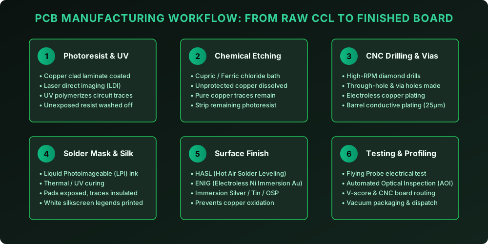
Raw copper-clad laminate is thoroughly cleaned and laminated with a photosensitive dry-film resist. A laser direct imaging system scans CAD vector data directly onto the photoresist with ultra-violet light, curing the exact geometry of the traces and copper pads.
The panel is sprayed with an alkaline or ferric chloride chemical etchant. The exposed, uncured copper is dissolved away, leaving behind only the protected copper traces. The hardened photoresist is subsequently stripped in an aqueous potassium hydroxide solution.
Computer-controlled spindle drills spinning at up to 200,000 RPM drill via and component holes. Because the bare drilled fiberglass hole walls are non-conductive, panels undergo an electroless chemical bath that deposits a microscopic seed layer of copper onto the barrel walls, followed by electroplating to build up 25 µm of solid copper.
To prevent bare copper pads from oxidizing before soldering, a surface finish is applied. Options include:
- HASL (Lead / Lead-Free): Dip in molten solder followed by hot air knives. Economical and rugged.
- ENIG (Electroless Nickel Immersion Gold): 3-5 µm nickel barrier capped with 0.05 µm pure gold. Ultra-flat planar surface essential for fine-pitch BGA packages.
- OSP (Organic Solderability Preservative): Water-based organic chemical film that evaporates during reflow.
Common PCB Failure Modes & How to Prevent Them
❌ Acid Traps in 90° Acute Angles
Problem: When traces turn at sharp 90-degree angles or form acute corners (< 90°), etching chemicals pool in the corner and continue eating away at the copper after the rinse stage, resulting in thinned traces or open circuits.
Solution: Always route traces with 45-degree chamfers or smooth arc radii.
❌ Tombstoning of SMD Passives
Problem: During reflow soldering, if one pad of an 0402 or 0603 capacitor is connected directly to a massive solid ground plane while the other connects to a thin trace, the ground pad acts as a heat sink. The solder on the thin trace melts first, exerting surface tension that pulls the component upright like a tombstone.
Solution: Apply thermal relief spokes on all component pads connected to large copper planes to balance thermal mass.
❌ Undersized Power Traces & Excessive Voltage Drop
Problem: Routing 3A to 5A motor driver or battery power rails with default 10-mil signal traces leads to significant $I^2R$ resistive heating, thermal delamination, and severe voltage sag.
Solution: Calculate required trace widths using IPC-2152 standards or use polygon copper pours (refer to our Trace Width Guide).
PCB Prototyping & Electronic Component Sourcing in India
For electronics engineers, hardware startups, and engineering students across India, rapid prototyping relies on a combination of online domestic PCB fabrication houses (like PCB Power, LionCircuits, JLCPCB India shipping) and local electronics markets for discrete components, soldering stations, and passives:
Bangalore
SMD passives, breakout modules, custom single-side PCB etching, test equipment
Mumbai
Power electronics, microcontrollers, heatsinks, industrial relays, chassis hardware
Delhi NCR
Wholesale semiconductors, transformers, custom PCB fabrication agents, power supplies
Chennai
Active ICs, sensors, STM32 / ESP32 modules, precision soldering tools
Hyderabad
Embedded development kits, passive components, prototyping zero-boards
Pune
Industrial automation breakouts, engineering lab consumables, connectors
Kolkata
Prototyping boards, solder wire, motors, through-hole and SMD discrete parts
Frequently Asked Questions
What is the full form and primary purpose of a PCB?
PCB stands for Printed Circuit Board. Its core purpose is to provide both mechanical support and reliable electrical connectivity to electronic components using conductive copper traces etched onto non-conductive insulating substrates.
Why is FR-4 the most common substrate material used in PCBs?
FR-4 (Flame Retardant 4) combines woven fiberglass cloth with an epoxy resin binder. It is the global standard because it provides excellent mechanical strength, flame retardancy (UL94V-0 compliant), high dielectric breakdown voltage, and dimensional stability at low manufacturing cost.
What does "1 oz copper" mean in PCB specifications?
One ounce (1 oz) copper means exactly one ounce of copper rolled evenly over a surface area of one square foot. This translates to an exact physical foil thickness of approximately 35 micrometers (µm) or 1.37 mils (0.00137 inches).
What is the difference between a Through-Hole Via, Blind Via, and Buried Via?
A Through-Hole Via spans entirely from the top layer to the bottom layer. A Blind Via connects an outer layer to one or more internal layers without penetrating the entire board. A Buried Via connects internal layers only and is invisible from either external surface.
Why is green the most common solder mask color?
Green solder mask was historically adopted by military contracts because it provided the highest visual contrast for human inspectors inspecting copper traces and identifying solder bridges under industrial inspection lamps. It also yields the highest resolution and thinnest application tolerance.
What is the difference between HASL and ENIG surface finishes?
HASL (Hot Air Solder Leveling) coats exposed copper in molten tin-lead or lead-free solder leveled by hot air knives; it is economical but produces uneven pad topography. ENIG (Electroless Nickel Immersion Gold) deposits an ultra-flat planar layer of nickel and gold, ideal for fine-pitch BGA packages and long shelf life.
What is the purpose of silkscreen on a PCB?
The silkscreen layer applies non-conductive epoxy ink on top of the solder mask to print alphanumeric component designators (e.g., R1, C1, U1), polarity indicators, test point identifiers, warning symbols, and manufacturing revision numbers for assembly and debugging.
Conclusion: Mastering PCB Fundamentals
Understanding how printed circuit boards work bridges the critical gap between theoretical circuit schematics and physical, high-reliability hardware. By selecting appropriate substrate materials, calculating trace cross-sections, and adhering to manufacturing design rules (DFM), engineers ensure their designs transition smoothly from digital CAD files to mass production.
Continue exploring our companion guides on PCB Design Step-by-Step and 4-Layer Stackup Architecture to take your hardware engineering skills to the professional level.
📚 References & Authoritative Standards
Related Hardware & PCB Guides
How to Design a PCB
From schematic capture to Gerber file generation step-by-step.
PCB Trace Width Guide
IPC-2152 formulas for current capacity and thermal rise calculations.
4-Layer PCB Stackup
Layer ordering, ground return paths, and EMI suppression.
Flex PCB vs Rigid PCB
Polyimide vs FR-4 comparison, bend radius formulas and dynamic flex rules.