What is PCB Trace Width & Current Carrying Capacity?
- [Copper Cross-Section Area] [dictates] [maximum continuous current capacity and thermal rise]
- [IPC-2152 Standard] [models] [heat dissipation into surrounding FR-4 dielectric and ground planes]
- [Undersized PCB Traces] [cause] [excessive resistive voltage sag, thermal delamination, and catastrophic trace fusion]
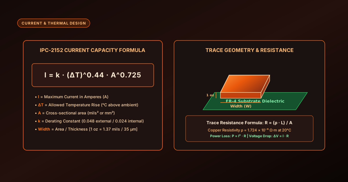
Every copper trace on a printed circuit board functions as a physical resistor with a finite resistance determined by the resistivity of copper (ρ = 1.724 × 10⁻⁸ Ω·m), trace length (L), and cross-sectional area (A = Width × Thickness).
When electrical current flows through a trace, power is dissipated as heat according to Joule's Law: P = I² · R. If the rate of heat generation exceeds the rate at which heat can dissipate into the surrounding air and FR-4 substrate, the temperature of the trace climbs rapidly. In severe overcurrent situations, the temperature can exceed the glass transition temperature (Tg) of the FR-4 epoxy (~130°C–170°C), causing the copper foil to blister, delaminate, and vaporize like a fuse.
IPC-2152 Mathematical Formula & Step-by-Step Derivation
The international industry standard for calculating current capacity in printed circuit boards is IPC-2152. The foundational empirical formula relating current, allowable temperature rise, and trace cross-sectional area is:
Where I is Current (Amperes), ΔT is Temperature Rise (°C), A is Cross-Sectional Area (mils²), and k is the Derating Constant.
External Layers (k = 0.048)
External traces benefit from air convection and thermal radiation through thin solder mask. They carry roughly 2x more current than an internal trace of the same width for the same temperature rise.
Internal Layers (k = 0.024)
Internal traces are trapped inside fiberglass epoxy (k_thermal ≈ 0.25 W/m·K). Because epoxy acts as a thermal blanket, the derating constant k drops by 50% (0.024).
Solving for Required Trace Width (W):
- Step 1: Calculate Required Cross-Sectional Area (A in mils²):A = [ I / (k · (ΔT)^0.44) ]^(1 / 0.725) = [ I / (k · (ΔT)^0.44) ]^1.379
- Step 2: Calculate Trace Width (W in mils):W = A / (Thickness × 1.378) [where Thickness is in oz/ft², e.g., 1 oz = 1.37 mils]
- Step 3: Convert to Millimeters:W_mm = W_mils × 0.0254
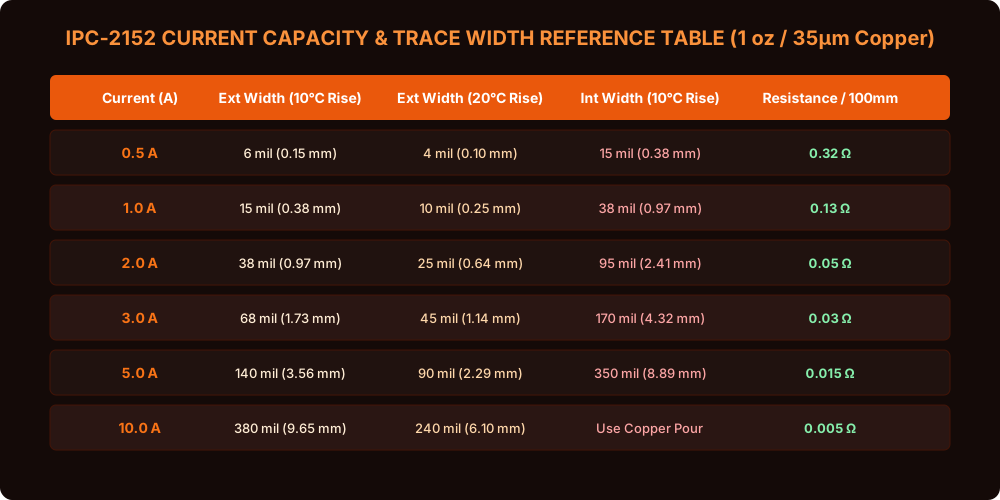
IPC-2152 Quick Lookup Table (1 oz / 35 µm Copper)
Use this engineering reference table for quick design sizing on standard 1 oz (35 µm) copper boards:
Copper Thickness & Weight Reference
| Copper Weight (oz/ft²) | Thickness in Micrometers (µm) | Thickness in Mils (thou) | Typical Application |
|---|---|---|---|
| 0.5 oz (18 µm) | 17.5 µm | 0.68 mil | Fine pitch BGA, smartphone HDI, low-current signals |
| 1.0 oz (35 µm) | 35.0 µm | 1.37 mil | Universal standard for 90% of microcontrollers & IoT boards |
| 2.0 oz (70 µm) | 70.0 µm | 2.74 mil | Motor drivers, 10A buck converters, drone ESCs |
| 3.0 oz (105 µm) | 105.0 µm | 4.11 mil | High-power industrial inverters, EV battery management (BMS) |
| 4.0 oz (140 µm) | 140.0 µm | 5.48 mil | Extreme heavy copper, high-power DC distribution bus boards |
High-Current Layout Techniques: Beyond Standard Traces
When a circuit must handle 10A, 20A, or 50A continuous current (such as in motor controllers, BLDC ESCs, and battery packs), standard trace widths become impossibly wide (10mm – 30mm). Engineers utilize these advanced hardware layout strategies:
1. Solder Mask Windows & Solder Bumping
Remove the solder mask over the high-current trace to expose bare copper. During wave soldering or hand assembly, a thick layer of 60/40 or lead-free solder is flowed over the copper track. Because solder has a bulk resistivity only ~8x higher than copper, adding a 1mm thick solder bead increases effective current capacity by 300% to 500% without widening the trace.
2. Paralleling Traces with Stitched Via Arrays
Route duplicate wide traces on both Top and Bottom copper layers (or across internal power planes in a 4-layer PCB stackup). Connect the parallel tracks with a dense grid of 0.3mm vias. A single 0.3mm drill via with 25µm copper barrel plating safely carries ~1.5A to 2.0A. A grid of 10 stitched vias carries up to 15A with minimal thermal gradient.
3. Solid Copper Bus Bars & Surface Mount Jumpers
For currents exceeding 30A (e.g., electric vehicle battery connections), solid tin-plated copper bus bars or heavy-gauge 12 AWG solid copper wire is soldered directly across the exposed PCB trace pads, shunting 90% of the current through the low-resistance solid conductor.
Heavy Copper PCB Fabrication & Thermal Testing in India
Indian hardware builders sourcing 2 oz / 3 oz heavy copper PCBs, high-current connectors (XT60, XT90, Anderson Powerpole), and thermal imaging cameras can procure from local electronics hubs:
Bangalore
Heavy copper 2oz/3oz prototype fabrication, FLIR thermal camera rentals, high-amperage terminal blocks
Mumbai
High-current MOSFET drivers (TO-247, D2PAK), extruded aluminum heatsinks, heavy copper bus bars
Delhi NCR
SMPS transformer winding, heavy current shunt resistors (1mΩ / 5W), high-power PCB batch assembly
Chennai
Automotive wiring harnesses, high-voltage isolation optocouplers, XT60/XT90 connectors
Hyderabad
EV motor controller prototyping components, battery spot welders, thermal interface pads (TIM)
Pune
Industrial drive electronics, heavy copper multi-layer board manufacturers, dyno test equipment
Kolkata
Heavy-gauge enameled copper wire, solder paste tubs, high-wattage ceramic wirewound resistors
Frequently Asked Questions
Why do internal PCB traces have less current-carrying capacity than external traces?
External copper traces are exposed to ambient air and convection cooling (plus solder mask radiation), which dissipates heat rapidly. Internal traces are completely encapsulated within FR-4 dielectric epoxy, a thermal insulator (thermal conductivity ~0.25 W/m·K), causing heat to become trapped. As a result, internal traces require roughly double the cross-sectional area for the same current and temperature rise.
What is the IPC-2152 formula for PCB trace current capacity?
The foundational formula is I = k · (ΔT)^0.44 · A^0.725, where I is maximum current in Amperes, ΔT is the allowable temperature rise above ambient in °C, A is the cross-sectional area in mils², and k is a derating constant (0.048 for external layers, 0.024 for internal layers).
How thick is 1 oz vs 2 oz copper on a PCB?
1 oz copper corresponds to 1 ounce of copper per square foot, resulting in a thickness of 35 µm (1.37 mils / 0.035 mm). 2 oz copper is twice as thick at 70 µm (2.74 mils / 0.070 mm). Using 2 oz copper cuts trace resistance and heat generation in half for the exact same trace width.
How do you calculate trace resistance and voltage drop?
Resistance is calculated using R = (ρ · L) / A, where ρ is the resistivity of copper (1.724 × 10⁻⁸ Ω·m), L is trace length, and A is cross-sectional area. Voltage drop is calculated using Ohm's Law: ΔV = I · R. For example, a 100mm long, 1mm wide trace on 1 oz copper has approximately 0.049 Ω resistance and drops 0.245V at 5A.
What techniques can I use to handle 10A to 30A on a standard PCB?
To carry extreme currents without massive trace widths: (1) Use wide polygon copper pours instead of thin traces; (2) Upgrade the board to 2 oz or 3 oz heavy copper; (3) Route identical parallel power traces across multiple layers connected with dense stitched via arrays; (4) Leave solder mask openings over the high-current trace and manually add thick solder bead bridges or solder solid copper bus wires directly on top.
What is the difference between IPC-2221 and IPC-2152 standards?
IPC-2221 was published in the 1950s/1990s based on legacy military charts that assumed isolated traces on uncoupled polyimide boards with no thermal planes. IPC-2152 is the modern, experimentally validated standard (released in 2009) that accounts for board thickness, copper plane heat sinking, component density, and modern FR-4 materials, providing vastly more accurate current limits.
What trace width should I use for general 3.3V and 5V digital signals?
For low-current digital logic signals (microcontroller GPIOs, I2C, SPI, UART) carrying microamps to a few milliamps, a standard trace width of 6 mil to 10 mil (0.15 mm – 0.25 mm) is standard, easy for PCB fabrication houses to etch, and provides excellent signal density.
Conclusion: Designing Reliable Power Distribution Systems
Precision trace width calculation is the bedrock of safe and robust electronic hardware. By applying IPC-2152 formulas, selecting appropriate copper weights (1 oz vs 2 oz), and utilizing copper pours and via stitching for high-amperage nodes, you eliminate unexpected brownouts, prevent thermal runaway, and ensure long operating lifespans for your circuits.
📚 References & Authoritative Thermal Standards
Related Hardware & PCB Guides
How PCB Works
Anatomy, copper foils, FR-4 substrate, and manufacturing steps.
How to Design a PCB
Step-by-step EDA guide from schematic to Gerber export.
4-Layer PCB Stackup
Plane distribution, ground return paths, and low-impedance power routing.
Flex PCB vs Rigid PCB
Flexible circuit bend rules, coverlay, and dynamic mechanical flexing.